 Featured
Hackathons
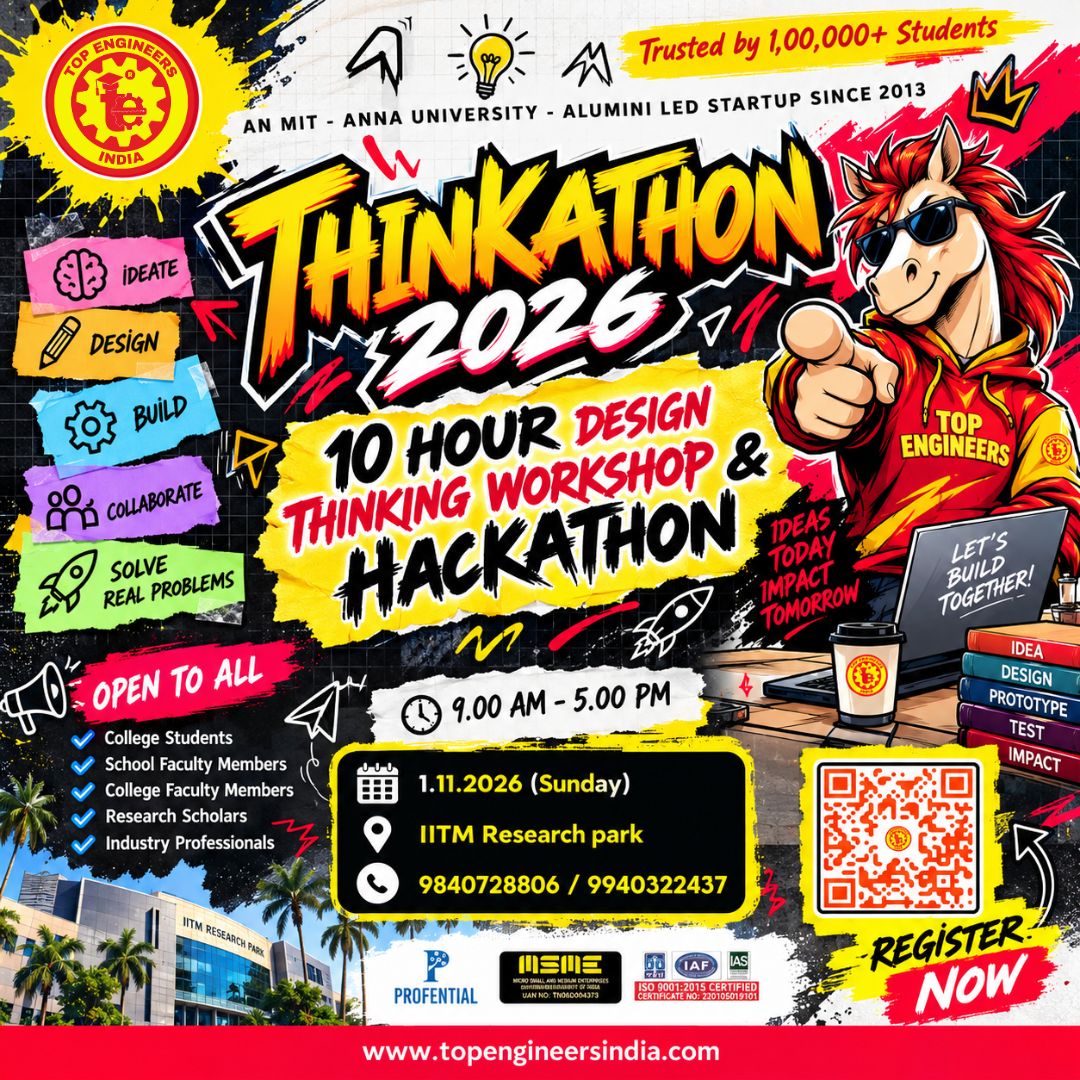
(Thinkathon 2026) - 10 Hour Design Thinking Workshop & Hackathon
01 Nov 2026 · Chennai
View event ↗DISCOVER · CONNECT · TAKE PART
Hosted by Top Engineers
PRINTED CIRCUIT BOARD DESIGN WORKSHOP (PCB - 2019) ORGANIZED BY TOP ENGINEERS ( A MIT- ANNA UNIVERSITY ALUMNI START UP) under the auspices of
TOP INTERNATIONAL EDUCATIONAL TRUST
VENUE IIT MADRAS RESEARCH PARK
No.32, Kanagam Rd, KanagamPeriyar Nagar, Taramani, Chennai, Tamil Nadu 600113.
(IITM Research park is only a venue and the event is organized by TOPENGINEERS only)
FOR REGISTRATION https://www.topengineers.co.in/register.php
REGISTRATION FEES
CERTIFICATE FROM TOP ENGINEERS WITH ISO CERTIFIED NUMBER AND HOLOGRAM WILL BE PROVIDED BY THE END OF THE WORKSHOP WHICH WILL ADD VALUE DURING PLACEMENTS.
INR 900/- PER PERSON (INDIA) (including GST)
$100 USD ( FOR OTHER COUNTRIES)
GROUP DISCOUNT OFFER
Group of 5 & above will get 5% Discount
Group of 10 & above will get 10% Discount
DATE 25.8.2019 (SUNDAY)
ABOUT TOPENGINEERS TOP ENGINEERS is an organization which is run by MIT-ANNA UNIVERSITY ALUMNI, Chennai. TOP ENGINEERS specializes in providing hands on experience on industrial practices to its participants through various workshops, seminars and other means by renowned subject matter experts and researchers to bring out the real world experience.TOP ENGINEERS workshops are designed to provide an insight view in the field of engineering.All the concepts will be explained in detail with the help of practical and with specially designed animations which would help the students to visualize things before actually practically working on it. TOP ENGINEERS have conducted more than 500 programs in India and trained over 1, 00,000+ students in the last 7 years.
AGENDA MORNING
SESSION INTRODUCTION
PCB BOARDS
EAGLE CAD SOFTWARE
DESIGNING OF SYMBOLS
DESIGNING SCHEMATICS
DESIGNING PACKAGE
DESIGNING COMPONENTS FOOTPRINT
THROUGH HOLE
SURFACE MOUNT (SMD)
AFTERNOON SESSION DESIGNING PCB LAYOUT
THROUGH HOLE
SURFACE MOUNT
CREATING GERBER FILE FOR MANUFACTURING
Note: LAPTOP is Mandatory, since this is designing workshop
Printed Circuit Board Design Workshop PCB 2019
PCB Workshop
Printed Circuit Board Design Workshop PCB 2019
23.8.2019
INR 900/- PER PERSON (INDIA) (including GST)
$100 USD ( FOR OTHER COUNTRIES)
GROUP DISCOUNT OFFER
Group of 5 & above will get 5% Discount
Group of 10 & above will get 10% Discount
IIT MADRAS RESEARCH PARK
No.32, Kanagam Rd, KanagamPeriyar Nagar, Taramani, Chennai, Tamil Nadu 600113.
(IITM Research park is only a venue and the event is organized by TOPENGINEERS only)
NO
No published reviews yet. Share your experience of this event.
Featured
01 Nov 2026 · Chennai
View event ↗ Featured
 Featured
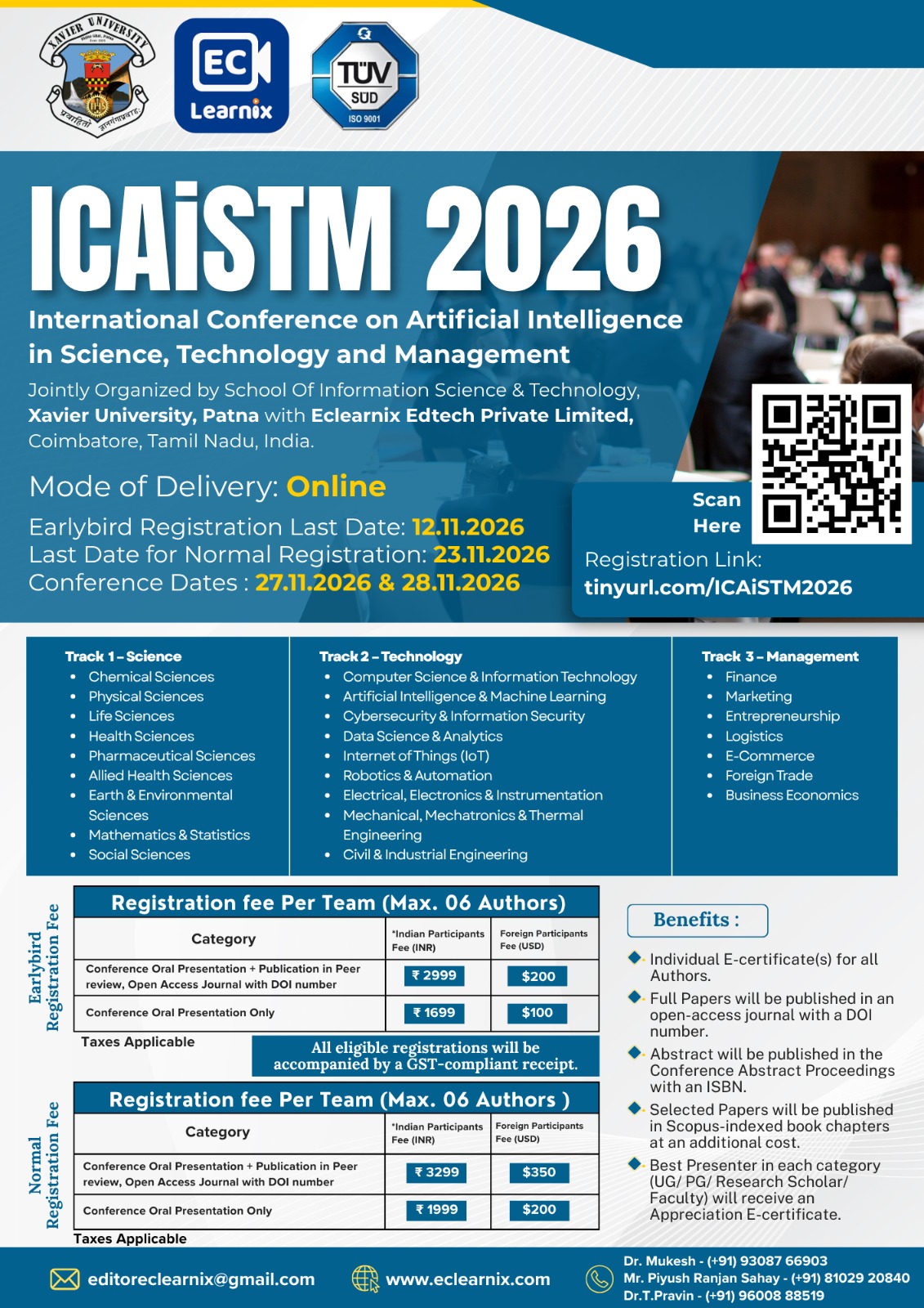
27 Nov 2026 · Online
View event ↗Explore more upcoming events like this.