 Featured
About the event
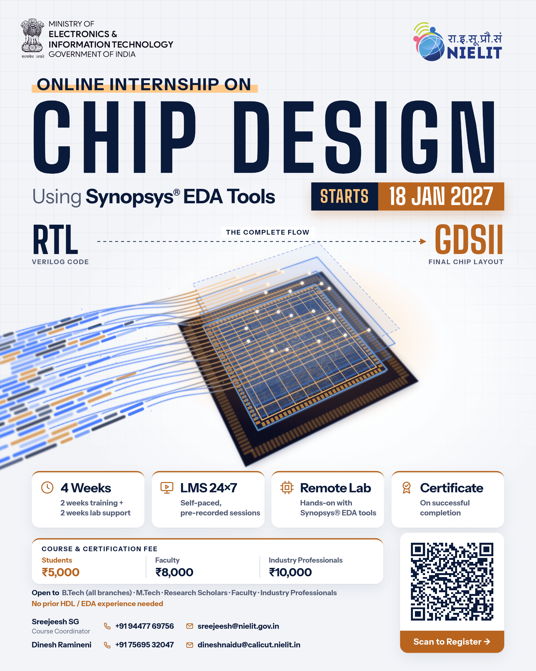
Online Internship on Chip Design Using Synopsys® EDA Tools
Organised by: National Institute of Electronics and Information Technology (NIELIT), Calicut
Ministry of Electronics & Information Technology, Government of India
About the Programme
The Online Internship on Chip Design Using Synopsys® EDA Tools is a four-week technical training programme designed to introduce participants to the complete ASIC design flow, from RTL development to the final GDSII layout database.
The programme consists of two weeks of structured training followed by two weeks of remote laboratory support. Participants will gain practical exposure to digital design using Verilog HDL, functional simulation, code coverage, logic synthesis, physical design, static timing analysis and physical verification.
The training begins with digital design and synthesis using Xilinx Vivado and progresses to industry-standard Synopsys® EDA tools for ASIC implementation.
Programme Highlights
- Four-week structured online internship.
- Two weeks of technical training.
- Two weeks of remote laboratory support.
- Self-paced, pre-recorded learning materials available 24×7 through LMS.
- Hands-on experience with Synopsys® EDA tools.
- Practical exposure to RTL-to-GDSII design flow.
- Independent mini-project during the laboratory phase.
- Certificate upon successful completion.
Technical Topics
- Introduction to RTL-to-GDSII Design Flow
- Digital Logic Design using Verilog HDL in Vivado
- Digital Logic Synthesis using Vivado
- Simulation using VCS®
- Coverage using VCS®
- Logic Synthesis using Design Compiler®
- Floorplanning and Power Planning using IC Compiler II™
- Placement and Clock Tree Synthesis using IC Compiler II™
- Routing and Sign-off using IC Compiler II™
- Static Timing Analysis using PrimeTime®
- Physical Verification using IC Validator™
Eligibility
- B.Tech students (all branches), including ongoing and passed-out students
- M.Tech students
- Faculty members
- Industry professionals
- Research scholars
No prior Verilog HDL or EDA tool experience is required. Basic knowledge of Linux, scripting and digital circuit design is recommended.
Duration and Mode
- Duration: 4 Weeks (20 Working Days)
- Mode: Online
- Learning Platform: LMS (24×7 access)
- Laboratory: NIELIT Calicut Remote Hardware Lab
Course and Certification Fee
- Students: ₹5,000
- Faculty: ₹8,000
- Industry Professionals: ₹10,000
Certification
Participants who successfully complete the programme, including the assigned project and online exit test, will receive a certificate.
Course Coordinator:
Sreejeesh SG
Senior Technical Officer, VLSI Lab
NIELIT Calicut
Registration:
https://www.calicut.nielit.in/OnlineCourseRegistration.aspx?c=OITP_VLSI_B3%2F2026%2F12%2F07
Who can join
Open to all
Additional eligibility details
Eligible Participants - B.Tech students (all branches), both ongoing and passed out - M.Tech students - Faculty members - Research scholars - Industry professionals Prerequisites - Basic knowledge of Linux - Basic knowledge of any scripting language - Knowledge of digital circuit design No prior Verilog HDL or EDA tool experience is required.
What’s on the agenda
Programme Schedule
Duration: 4 Weeks | 20 Working Days
Week 1 – Verilog HDL, Simulation and Logic Synthesis
Day 1: HDL Language and ASIC Design Flow
- Introduction to hardware description languages and ASIC design flow
- Structure of a Verilog module and basic fundamentals
Day 2: Verilog HDL, Hierarchy and Testbench Design
- Hardware design methodologies
- Hierarchical architecture
- Testbench architecture, simulation structure, clock and reset generation
Day 3: Tasks, Functions and Finite State Machines
- Verilog tasks and functions in behavioural modelling
- FSM fundamentals, states and transitions
Day 4: Simulation and Coverage using VCS®
- VCS® simulation flow, scripts, waveform generation and debugging
- Introduction to code coverage and coverage report interpretation
Day 5: Logic Synthesis using Design Compiler®
- Design Compiler environment and setup
- Technology library configuration and timing constraints
- Tcl scripting, RTL synthesis and synthesis report analysis
Week 2 – Physical Design and Verification
Day 6: Floorplanning and Power Planning using IC Compiler II™
- Physical-design data setup and floorplanning concepts
- Power-distribution planning and validation
Day 7: Placement and Clock Tree Synthesis
- Standard-cell placement and optimisation
- Congestion and timing considerations
- Clock buffers, insertion delay, skew and clock transition
Day 8: Routing and Sign-off
- Routing concepts and flow
- Sign-off and review of physical-design outputs and reports
Day 9: Static Timing Analysis using PrimeTime®
- STA fundamentals and PVT variation
- Standard-cell timing and timing paths
- Timing parameter analysis
Day 10: Physical Verification using IC Validator™
- Design Rule Checking (DRC)
- Layout Versus Schematic (LVS)
Weeks 3 & 4 – Remote Laboratory and Mini Projects
- Independent execution of the complete RTL-to-GDSII design flow on an assigned design
- Simulation, synthesis and physical implementation
- Development and execution of participant-written scripts
- Completion of the final layout database and associated deliverables
Final Assessment
- Online MCQ-based exit test
- Project deliverable submission
- Project evaluation and certification
Events & highlights
Key Highlights
- Complete RTL-to-GDSII ASIC Design Flow
- 2 Weeks of Structured Technical Training
- 2 Weeks of Remote Laboratory Support
- Hands-on Training with Synopsys® EDA Tools
- Verilog HDL Design and Functional Verification
- Logic Synthesis using Design Compiler®
- Physical Design using IC Compiler II™
- Static Timing Analysis using PrimeTime®
- Physical Verification using IC Validator™
- Independent Mini-Project
- 24×7 Self-Paced LMS Access
- Certificate upon Successful Completion
Event type details
Four-week online technical internship comprising two weeks of structured training and two weeks of remote laboratory support, covering the complete RTL-to-GDSII ASIC design flow using Synopsys® EDA tools.
Event Theme
VLSI Design, ASIC Implementation and Semiconductor Technology
Registration deadline / Important dates
Programme Start Date: 18 January 2027
Programme Duration: 4 Weeks
Mode: Online – LMS and Remote Hardware Lab
Registration: Through the official NIELIT registration portal.
Registration Fees
Course and Certification Fee
- Students: ₹5,000
- Faculty Members: ₹8,000
- Industry Professionals: ₹10,000
The applicable fee depends on the participant category. Registration and payment are through the official NIELIT portal.
How to Reach
Online Participation
This is an online internship programme. Participants can access course materials and pre-recorded sessions through the NIELIT Learning Management System (LMS), available 24×7.
During the laboratory phase, participants will receive access to the NIELIT Calicut Remote Hardware Lab to gain hands-on experience with Synopsys® EDA tools.
Registered participants will be provided with the necessary course and laboratory access instructions through the official LMS.
No physical attendance at the NIELIT Calicut campus is required for the online programme.
Contact the organizer
Sign in to view the organizer’s contact details.Sign in to view contacts ↗
Event reviews
No published reviews yet. Share your experience of this event.